A miniaturized sensor that can measure chemistry on a chip
By Bill Steele
By combining expertise in photonics – manipulating light beams in nanoscale waveguides on a chip – and materials science, Cornell researchers have laid the groundwork for a chemical sensor on a chip that could be used in small portable devices to analyze samples in a lab, monitor air and water quality in the field and perhaps even detect explosives.
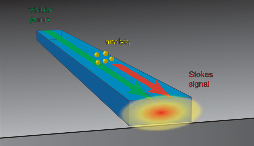
The researchers use a phenomenon called “Raman scattering:” When a laser strikes a molecule it kicks back the energy as photons of light at a variety of wavelengths that depend on the structure and composition of the molecule.
If a laser is fired into a waveguide – a tube of transparent material set into a silicon chip – the light bounces off the inside surfaces and is confined to the waveguide. But when the waveguide is only a few nanometers high, it’s smaller than the light waves, which spread out beyond he guide to create a so-called “evanescent field” above the surface of the chip. The beam can induce Raman scattering in the air above the chip, or in a drop of liquid placed on its surface for analysis. Light emitted by the excited molecules also follows the waveguide; a prism at the end of the waveguide can spread that light into a spectrum that is a “fingerprint” identifying the molecule that produced it.
“If you need a chemical sensor in the lab, that is not a problem,” said Jin Suntivich, assistant professor of materials science and engineering. “But finding a chemical sensor that you can take with you outside is a challenge. We want to develop a technology that is small enough to attach to a phone, so that your personal electronics can constantly monitor the world around you, and the moment you see something out of the ordinary, the sensor can tell you what it is.”
Sensors based on Raman scattering have been made before, using silicon nitride waveguides. With a few changes, the Cornell researchers have come up with a design that could make a sensor more sensitive and small enough to be used in the field.
“We’re not the first but we’re the best,” said Christopher Evans, a Kavli Postdoctoral Fellow in the Laboratory of Atomic and Solid State Physics and the Kavli Institute at Cornell for Nanoscale Science. Evans is first author of a paper describing the new approach published in the July 14 online edition of the American Chemical Society journal ACS Photonics. Co-authors are Suntivich and Chengyu Liu, a Ph.D. student in the School of Applied and Engineering Physics.

he first important change was to use waveguides of titanium dioxide in place of silicon nitride. Titanium dioxide has a much higher refractive index, making a greater contrast with the space above the chip, which creates a stronger evanescent field. The material is also transparent to light at visible wavelengths where Raman scattering is more pronounced. In silicon nitride, visible light generates an interfering luminescence. In early experiments, the researchers used a green laser pointer as a light source.
For a future device, a tiny laser can be built into a chip, as can a prism or some other mechanism to spread out the wavelengths of the Raman spectrum, and a photosensitive device to read it. One possibility is to read the spectrum with the camera in a phone.
Interaction of the pumping laser with the material above the chip increases with the length of the waveguide. To increase the interaction without making the chip unacceptably large, the researchers incorporated a “ring resonator.” When a circular waveguide is set tangent to a straight guide, some of the light will enter the ring and continue to circle around it, letting the light interact continually with the material above the chip. The circumference of the ring can be adjusted to resonate with the wavelength of the light, intensifying the effect. “We have shown that we can increase the amount of peak signal from our sensors by an order of magnitude or more, while simultaneously reducing the device footprint down to the cross-section of a human hair,” Evans said.
Potential applications include portable sensors to monitor air and water quality or conduct laboratory tests in the field. Chemists could observe chemical reactions while they occur.
The work was supported in part by the Cornell Center for Materials Research and used the Cornell Nanoscale Facility, both funded by the National Science Foundation. Additional support was provided by the Samsung Advanced Institute of Technology and the Kavli Institute at Cornell for Nanoscale Science.
Media Contact
Get Cornell news delivered right to your inbox.
Subscribe